Theory of Operation
Block Diagram
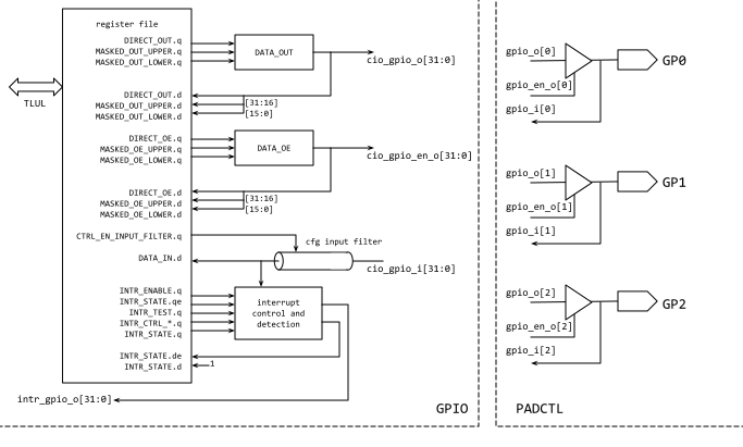
The block diagram above shows the DATA_OUT and DATA_OE registers
managed by hardware outside of the auto-generated register file.
For reference, it also shows the assumed connections to pads in
the top level netlist.
Design Details
GPIO Output logic
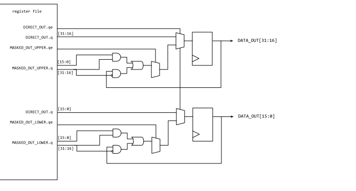
The GPIO module maintains one 32-bit output register DATA_OUT with two
ways to write to it. Direct write access uses DIRECT_OUT, and
masked access uses MASKED_OUT_UPPER and
MASKED_OUT_LOWER. Direct access provides full write and read
access for all 32 bits in one register.
For masked access the bits to modify are given as a mask in the upper
16 bits of the MASKED_OUT_UPPER and
MASKED_OUT_LOWER register write, while the data to write is
provided in the lower 16 bits of the register write. The hardware updates
DATA_OUT with the mask so that the modification is done without software
requiring a Read-Modify-Write.
Reads of masked registers return the lower/upper 16 bits of the DATA_OUT
contents. Zeros are returned in the upper 16 bits (mask field). To read
what is on the pins, software should read the DATA_IN register.
(See GPIO Input section below).
The same concept is duplicated for the output enable register DATA_OE.
Direct access uses DIRECT_OE, and masked access is available
using MASKED_OE_UPPER and MASKED_OE_LOWER.
The output enable is sent to the pad control block to determine if the
pad should drive the DATA_OUT value to the associated pin or not.
A typical use pattern is for initialization and suspend/resume code to
use the full access registers to set the output enables and current output
values, then switch to masked access for both DATA_OUT and DATA_OE.
For GPIO outputs that are not used (either not wired to a pin output or not selected for pin multiplexing), the output values are disconnected and have no effect on the GPIO input, regardless of output enable values.
Per-Pin Register View
In addition to the 32-bit registers, which group the GPIOs by function, the GPIO module provides a second register view that groups them by pin. This view allows assigning individual GPIOs to different software components, for example to CHERIoT compartments, by granting each component access to only the registers of its GPIOs. Both views alias the same state, and a write to a per-pin register only affects the GPIO it belongs to.
The per-pin view consists of two separate, aligned address ranges, so access to the data of a GPIO can be granted without access to its configuration:
PER_PIN_IOholds one register per GPIO with bit i ofDATA_OUTand ofDATA_IN.- The configuration range holds two registers per GPIO, which directly follow one another:
PER_PIN_OE_0with bit 0 ofDATA_OE,PER_PIN_INTR_CTRL_0with bit 0 of the interrupt control and input filter registers, thenPER_PIN_OE_1,PER_PIN_INTR_CTRL_1, and so on.
A register write must cover all bytes of the register that hold a field, so access cannot be granted to only some fields of a register. The output enable and the interrupt configuration of a GPIO are therefore in separate registers, so access to one can be granted without the other.
The interrupt registers INTR_STATE, INTR_ENABLE and INTR_TEST have no per-pin view.
Like the interrupt controller, they are expected to be managed by a trusted software component, for example a trusted CHERIoT compartment, which handles the GPIO interrupts on behalf of the components owning the GPIOs.
GPIO Input
The DATA_IN register returns the contents as seen on the
peripheral input, typically from the pads connected to those inputs. In the
presence of a pin-multiplexing unit, GPIO peripheral inputs that are
not connected to a chip input will be tied to a constant zero input.
The GPIO module provides optional independent noise filter control for each of the 32 input signals.
Each input can be independently enabled with the CTRL_EN_INPUT_FILTER (one bit per input).
This 16-cycle filter is applied to both the DATA_IN register and the interrupt detection logic.
The timing for DATA_IN is still not instantaneous if CTRL_EN_INPUT_FILTER is false as there is still both top-level routing delay and input CDC synchronizer delay involved.
The top-level routing delay depends on the physical layout of the chip.
The input synchronizer adds two flops between the chip input and the DATA_IN register, though the added delay may vary by up to one GPIO clock cycle depending on when cycle each external input transition arrives relative to the GPIO clock.
The contents of DATA_IN are always readable and reflect the value seen at the chip input pad regardless of the output enable setting from DATA_OE.
If the output enable is true (and the GPIO is connected to a chip-level pad), the value read from DATA_IN includes the effect of the peripheral’s driven output and will only differ from DATA_OUT if the output driver is unable to switch the pin or during the delay imposed by the input synchronizer and noise filter (if enabled).
GPIO Inputs as HW Straps
The GPIO controller provides an optional feature to sample GPIO input values as hardware configuration straps.
After each reset, on the first cycle when the strap_en_i signal is asserted, the GPIO detects its transition from low to high.
One clock cycle later, it samples the GPIO input values and stores them in the HW_STRAPS_DATA_IN register.
The strap_en_i signal transition from low to high is expected only once after the reset process.
Sampling occurs exclusively at this time, and any subsequent changes to the GPIO input configuration will not be captured.
This mechanism samples all 32 bits of the GPIO input data, regardless of the GPIO output enable status, providing a reliable snapshot of the input values for firmware access.
Interrupts
The GPIO module provides 32 interrupt signals to the main processor.
Each interrupt can be independently enabled, tested, and configured.
Following the standard interrupt guidelines in the Comportability
Specification,
the 32 bits of the INTR_ENABLE register determines whether the
associated inputs are configured to detect interrupt events. If enabled
via the various INTR_CTRL_EN registers, their current state can be
read in the INTR_STATE register. Clearing is done by writing a
1 into the associated INTR_STATE bit field.
For configuration, there are 4 types of interrupts available per bit,
controlled with four control registers. INTR_CTRL_EN_RISING
configures the associated input for rising-edge detection.
Similarly, INTR_CTRL_EN_FALLING detects falling edge inputs.
INTR_CTRL_EN_LVLHIGH and INTR_CTRL_EN_LVLLOW
allow the input to be level sensitive interrupts. In theory an input can be
configured to detect both a rising and falling edge, but there is no hardware
assistance to indicate which edge caused the output interrupt.
Note #1: The interrupt can only be triggered by GPIO input. Note #2: All inputs are sent through optional noise filtering before being sent into interrupt detection. Note #3: All interrupts to the processor are level interrupts as per the Comportability Specification guidelines. The GPIO module, if configured, converts an edge detection into a level interrupt to the processor core.