NOTE: This datasheet refers to Earl Grey 2, i.e., the second generation of the discrete OpenTitan chip design currently being developed on the master branch.
For the datasheet of the taped out Earl Grey design, i.e., the first production OpenTitan silicon, refer to the documentation for the earlgrey_1.0.0 branch available here.
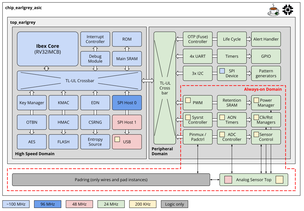
Earl Grey 2 is OpenTitan’s next-generation discrete secure microcontroller architecture.
Its primary goals are
- significantly enhanced support for hardened Post-Quantum Cryptography (PQC),
- support for next-generation I/O standards,
- support for implementation in recent silicon technologies, replacing embedded Flash and fuses with Resistive RAM (RRAM) as on-chip non-volatile memory, and
- support CHERIoT as switchable base ISA in addition to RV32I.
The OpenTitan Earl Grey 2 architecture supports the following key features:
| OpenTitan Earl Grey 2 Features |
- Ibex 32-bit RISC-V CPU core
(RV32{I,CHERIoT}MCB_Zicntr_Zicsr_Zifencei_
Zihpm_Zcb_Zcmp_Zbc_Zbkb_Zbkx_
Smepmp):
- 3-stage pipeline: instruction fetch, decode and execute, writeback
- RV32I base ISA: version 2.1, active after reset
- CHERIoT base ISA: version v1.0, can be switched to once (i.e., no way back to RV32I until reset)
- CHERIoT background revocation engine: sweeps the Main SRAM, the Secondary SRAM and the RRAM and clears the tag of every revoked capability
- M (integer multiplication and division) extension: version 2.0, single-cycle multiplier
- C (compressed instructions) extension: version 2.0
- ZcbZcmp (code size reduction) extensions: version 1.0.0
- Bit manipulation extensions:
- version 1.0.0 of Zba_Zbb_Zbs (B)
- version 1.0.0 of Zbc_Zbkb_Zbkc_Zbkx
- Smepmp: enhanced physical memory protection (ePMP) version 1.0, 16 entries, 4 byte minimum granularity
- Execution modes: M (machine), U (user)
- PLIC (platform level interrupt controller)
- Instruction cache:
- 4 KiB capacity
- 2-way set associative
- 64 instruction bit + 14 ECC bit per entry
- Hardware Security features:
- Dual-core lockstep configuration
- Integrity checks on register file (RF), instruction cache, and bus interfaces
- Hardened program counter (PC)
- Data-independent timing can be enabled in a CSR: Zkt extension plus branches
- Dummy instruction insertion
- Instruction cache scrambled with low-latency cipher
- Memories:
- 128 KiB Main SRAM
- intended use: general-purpose data (e.g., heap, stack) storage
- 32 data bit + 7 ECC bit per architectural row
- CHERIoT support: full address range usable to store CHERIoT capabilities that can be revoked at a granularity of 8 bytes
- CHERIoT implementation: tag bits (2 KiB) and revocation bits (2 KiB) stored in the CHERIoT meta SRAM
- scrambling of address and data with reduced-round PRINCE cipher
- hardened against FI attacks with a readback mechanism
- 64 KiB Secondary SRAM
- intended use: general-purpose data (e.g., heap, stack) storage
- 32 data bit + 7 ECC bit per architectural row
- CHERIoT support: full address range usable to store CHERIoT capabilities that can be revoked at a granularity of 8 bytes
- CHERIoT implementation: tag bits (1 KiB) and revocation bits (1 KiB) stored in the CHERIoT meta SRAM
- scrambling of address and data with reduced-round PRINCE cipher
- hardened against FI attacks with a readback mechanism
- 8 KiB Always-On (AON) Retention SRAM
- intended use: retain data during deep sleep
- 32 data bit + 7 ECC bit per architectural row
- scrambling of address and data with reduced-round PRINCE cipher
- hardened against FI attacks with a readback mechanism
- 2 MiB on-chip non-volatile memory (RRAM)
- 128 data bit per architectural row
- vendor-implemented ECC
- scrambling of address and data with XEX tweakable block cipher
- OTP emulation
- CHERIoT support: full address range usable to store CHERIoT capabilities that cannot be revoked; a capability store sets the tag of a capability the RRAM already holds
- CHERIoT implementation: tag bits (32 KiB) stored in the CHERIoT meta SRAM
- 2 KiB one-time programmable (OTP) memory (stored in RRAM)
- logically partitioned with support for scrambling, read locking, write locking, integrity protection, and zeroization
- 192 KiB ROM for Ibex CPU
- scrambling of address and data with reduced-round PRINCE cipher
- 32 KiB OTBN data memory
- 256 data bit + 56 ECC bit per architectural row
- scrambling of address and data with reduced-round PRINCE cipher
- 16 KiB OTBN instruction memory
- 32 data bit + 7 ECC bit per architectural row
- scrambling of address and data with reduced-round PRINCE cipher
- 38 KiB CHERIoT meta SRAM
- This stores the CHERIoT tag and revocation bits for the Main SRAM and the Secondary SRAM and the CHERIoT tag bits for the RRAM.
- 32 data bit + 7 ECC bit per architectural row.
- In CHERIoT mode, this SRAM is only accessible by software as far as required and permitted by the CHERIoT specification.
- In non-CHERIoT mode, this SRAM is not accessible by software.
- Scrambling of data with reduced-round PRINCE cipher; address scrambling is currently disabled.
- Hardened against FI attacks with a readback mechanism.
|
- Security hardware IP blocks:
- AES-128/192/256
- ECB/CBC/CFB/OFB/CTR modes in hardware
- GCM mode through software on Ibex
- key sideload interface from Key Manager
- first-order SCA masking
- FI countermeasures on the control path
- SHA2/HMAC-256/384/512
- HMAC key length up to 1024 bit
- state save & restore (context switch)
- key sideload interface from Key Manager
- FI countermeasures on the control path
- KMAC/SHA3-224/256/384/512/[c]SHAKE-128/256
- KMAC key length up to 512 bit
- state save & restore (context switch) only on SW interface
- key sideload interface from Key Manager
- first-order SCA masking
- FI countermeasures on the control path
- OpenTitan Big Number Accelerator (OTBN)
- programmable accelerator for asymmetric cryptography including PQC, elliptic curve cryptography (ECC), and RSA
- key sideload interface from Key Manager
- supports hardened PQC (ML-DSA and ML-KEM) with SIMD instructions, masking accelerator (secure add and A2B/B2A mask conversions), and an interface to KMAC
- Entropy complex
- Entropy Source
- CSRNG with state save & restore (context switch)
- Entropy Distribution Network (EDN)
- Key Manager DPE
- supporting DICE including the DICE Protection Environment (DPE) extension
- attestation chain with four stages: UDS0, UDS1 (including seed provided by Silicon Owner, which is stored in OTP, as HW binding value), CDI0, and CDI1
- sealing chain with four stages (ladder advancements symmetrical to attestation chain)
- 4 internal key slots
- key sideloading to IPs:
- 512 bit to OTBN for PQC key material
- 512 bit to HMAC
- 256 bit to KMAC
- 256 bit to AES
- Alert Handler
- Life Cycle Controller
- IO hardware IP blocks:
- 2x I3C Controller + Target (on muxed pins, restricted pin sets, tightly controlled timing)
- Signaling modes: HDR-DDR (24 Mbps), SDR (12 Mbps)
- Programmed I/O (PIO) mode implementation of Host Controller Interface (HCI)
- Transfer Command Response Interface (TCRI)
- In-band interrupts (IBI)
- Message buffer: 1024 entries x 32 bit
- Device Address Table (DAT): 32 entries x 52 bit
- Device Characteristics Table (DCT): 32 entries x 72 bit
- Virtual targets: 2 (per instance)
- Extra output signal controlling external resistor for SDA pull-up in Controller mode
- 1x USB 2.0 Full-Speed (12 Mbps) Device (on fixed pins) with support for Test Packet mode and improved recovery from invalid traffic
- 2x SPI Host (1 on fixed pins, 1 on muxed pins)
- SPI Host 0:
- Quad SPI
- SCK at 48 MHz max (96 MHz internally)
- fixed pins
- 3 chip select (1 on fixed pin, 2 on muxed pins)
- Passthrough mode from SPI Device
- SPI Host 1:
- Quad SPI
- SCK at 48 MHz max (96 MHz internally)
- muxed pins (restricted pin sets, tightly controlled timing)
- 3 chip select (on muxed pins)
- 1x SPI Device (on fixed pins)
- Passthrough mode to SPI Host 0 on fixed pins
- 2 chip select (1 on fixed pin, 1 on muxed pin)
- 3x I2C (on muxed pins)
- 4x UART (on muxed pins)
- 32x GPIO (on muxed pins)
- Pin Multiplexer
- ADC Controller
- System Reset Controller
- Chip control hardware IP blocks:
- Clock, reset and power managers
- Fixed-frequency timers
- Always-On (AON) timer
- Software:
- Boot ROM code implementing secure boot and chip configuration
- Bare metal top-level tests
- OpenTitan Crypto Library with OTBN accelerated and security hardened algorithms for
- ML-DSA-87 Sign, Verify, Keygen
- RSA 2K, 3K, 4K
- ECDSA-{P256,P384}, ECDH-{P256,P384}, Ed25519, X25519
- ML-DSA-87 PQ-secure boot
|
- Non-volatile on-chip memory: Resistive RAM (RRAM)
- No OTP macro; OTP to be emulated by connecting OTP Controller to new RRAM Controller instead of an OTP macro
- Target frequency for main/fast clock domain: ~150 MHz
- I/O clock domains frequency:
- IO: 96 MHz
- IO_DIV2: 48 MHz
- IO_DIV4: 24 MHz
- USB: 48 MHz
- Always-on clock domain frequency: 200 kHz
For more detailed documentation including the pinout and system address map, see OpenTitan Earl Grey Chip Specification.
The OpenTitan Earl Grey Chip DV Document describes the chip-level DV environment and contains the chip-level test plan.