Integration Notes
These notes describe the integration of the I3C IP block. It is a split IP with two partitions, which the integration may place in different power domains:
- The primary partition,
i3c_part_primary, wraps the IP core,i3c_core, with the TL-UL register and memory interfaces, the alert sender and the CIO pins of the bus. - The secondary partition,
i3c_part_secondary, contains the Target Reset Detector.
IP Clock Frequency
In I3C terminology there are two types of I3C bus supported by this IP block. These are the ‘Mixed Fast Bus’ which incorporates both I2C targets and I3C Basic devices, and the ‘Pure Bus’ which supports only I3C devices.
The duration of the interval when Serial CLock (SCL) is driven high by the Active Controller is critical to the operation of an I3C ‘Mixed Fast Bus’. If the pulse is too long then the I3C traffic will not be suppressed by the spike filter of an I2C device on a ‘Mixed Fast Bus’ and it may cause malfunction of the I2C device. If it is too short then it may cause communication issues with I3C Targets.
The IP block offers a top-level design parameter ClkFreq which specifies the frequency in Hz of the main IP clock.
Additionally there are timing parameter registers presented to software which may then specify the duration of critical time intervals in units of the IP clock period.
| Pure Bus | Minimum | Maximum |
|---|---|---|
| High period of SCL Clock | 32 ns | N/A |
For a ‘Pure Bus’ there is no maximum duration for the SCL high interval, so any reasonable IP clock frequency may be accommodated simply by increasing the number of cycles for which SCL is driven high. A frequency range of 50 MHz (inclusive) to 1.5 GHz (inclusive) is supported by the IP block in this case, with frequencies down to 32 MHz (exclusive) also being supported at the cost of a proportionate decrease in the maximum signaling speed.
| Mixed Fast Bus | Minimum | Maximum |
|---|---|---|
| High period of SCL Clock | 32 ns | 41 ns |
Example clock frequencies and required tolerance:
| Clock frequency | Tolerance | SDR | HDR-DDR |
|---|---|---|---|
| 50 MHz | +/-2% | 11.1 Mbps | 20.0 Mbps |
| 55 MHz | +/-10% | 9.7 Mbps | 17.6 Mbps |
| 85 MHz | +/-9% | 10.8 Mbps | 19.4 Mbps |
As the above table shows there is a trade off between the frequency accuracy and the achievable data rates. Note that the quoted data rates are the effective rate of data transfer, assuming that read/write transfers are sufficiently large to mitigate the protocol overheads. The peak signaling rates are 12.5 Mbps for SDR and 25 Mbps for HDR-DDR.
It should also be observed that for frequencies between 50 MHz and 100 MHz there may be a requirement to reduce further the rate of data transfers to/from targets that have a large tSCO delay (time from SCL edge to SDA output).
This is because the Controller logic samples SDA an integral number of IP clock cycles after the SCL edge, and increasing the clock frequency extends the SCL low period to an odd number of clock cycles, moving the sampling points closer to the transitions on SCL.
Half-cycle SCL high extension
The IP block may be parameterized to support an extension of the SCL high pulse by half of the IP clock period. This increases the set of clock frequencies that may be used in deployments of the IP. The half-cycle extension is achieved by forming the SCL output signal of the Controller from contributions from two flip-flops, clocked on opposing edges of the IP clock.
| Clock frequency | Tolerance | SDR | HDR-DDR |
|---|---|---|---|
| 96 MHz | +/-11% | 10.6 Mbps | 19.2 Mbps |
The unavoidable combinational logic on the SCL output is kept as minimal as possible in the logical design and it is important at the physical level to ensure that this signal is free of glitches since SCL controls the I3C bus in its entirety.
Impact of SCL Clock Rise and Fall Times
It is important to note that the Active Controller always drives the SCL Clock signal in push-pull mode. In places the I3C Basic specification includes prose and diagrams that refer to ‘Open Drain Timing’, and it even employs the phrase ‘Open Drain SCL Low Period.’ These intervals require Open Drain driving of the SDA data lane(s), and the use of modified timing, but the SCL signal is still being driven in push-pull mode by the Active Controller.
With that cautionary note stated, it should be understood that the use of ‘Open Drain Timing’ on a ‘Mixed Fast Bus’ imposes a number of constraints on the SCL Clock rise time (tCR), high period (tHIGH) and fall time (tCF) in order to ensure compatibility with I2C devices. All of these constraints must be met simultaneously:
- SCL Clock Rise time (tCR) must be no more than 8 ns for maximum signaling frequency (fSCL = 12.5 MHz).
- SCL Clock Fall time (tCF) must be <= 8 ns also, again for 12.5 MHz signaling.
- SCL Clock High period (tHIGH) when employing ‘Open Drain Timing’ on a ‘Mixed Fast Bus’ must be <= 41 ns.
- SCL Clock High period when employing ‘Push-Pull Timing’ on a ‘Mixed Fast Bus’ (tDIG_H_MIXED) must be <= 45 ns.
- This ‘digital high’ period is defined as tHIGH + tCF (see Figure 75 of I3C Basic Version 1.2).
In order to satisfy all of these constraints, the duration of the SCL Clock High period may need to be shortened in order to ensure that I3C traffic remains invisible to I2C Targets. e.g. if only the worst case tCR and tCF can be met, tHIGH will need to be reduced accordingly to no more than 37 ns (45 ns - 8 ns).
The full details may be found in Tables 49 and 50 of the Specification for I3C Basic, Version 1.2.
I/O signals and driver styles
The IP block presents the I3C bus as two Chip I/O (CIO) pins, scl and sda, which the Controller and the Target share (see Hardware Interfaces):
cio_scl_i,cio_scl_oandcio_scl_en_o- Serial CLock (SCL). Only the Controller drives SCL, andcio_scl_en_ois asserted while it is the Active Controller.cio_sda_i,cio_sda_oandcio_sda_en_o- Serial DAta (SDA). The IP block combines the SDA drivers of the Controller and the Target onto these signals; at most one of them drives SDA at any time.
The Target Reset Detector in the secondary partition observes the bus through two further input pins, rstdet_scl and rstdet_sda (see Target Reset Detector).
Internally, the Controller and the Target present their driver outputs using SystemVerilog compound types from the package i3c_io_pkg, allowing the set of signals to be modified with reduced impact upon the RTL design.
Two implementations of this package are available, and only one of them shall be included in the build.
FuseSoC selects the Virtual Open Drain style by default, and the Separated Enables style when the flag i3c_io_sep_drv_en is set.
Separated Enables (rtl/io_sep/i3c_io_pkg.sv)
sda_pp_en- Push-pull enable forsda.sda_od_en- Open drain enable forsda.sda- Serial DAta line(s), gated bysda_pp_enandsda_od_en.
This style suits pad cells with separate push-pull and open drain enable inputs, which keep their pull-up transistor off for open drain signaling.
Virtual Open Drain (rtl/io_vod/i3c_io_pkg.sv)
sda_en- Enable(s) forsda. Asserted for push-pull low/high output and for open drain low output; deasserted for open drain high output.sda- Serial DAta line(s), gated bysda_en.
In this style the IP block performs open drain signaling itself: for an open drain high output, it deasserts sda_en, which turns off both pad transistors.
The pads shall therefore be configured for push-pull operation, with open drain and virtual open drain disabled.
Electrically, both styles produce the same signaling; they differ only in whether the pad cell or the IP block keeps the pull-up transistor off for open drain signaling.
In both styles the Controller additionally presents:
scl_en- Enable for the Serial CLock (SCL) output signal; its state depends upon whether the IP block is the Active Controller.scl- SCL output signal, gated byscl_en.
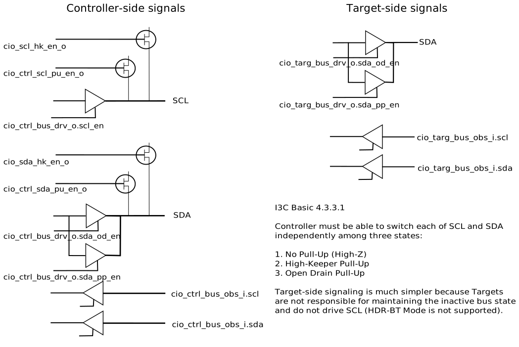
Pullups and high-keepers
In addition to the SCL and SDA signals and their respective enables, each of SCL and SDA must also support both a ‘high-keeper’ and a pullup resistance. The latter is required to ensure a defined state when open drain signaling is employed, e.g. during an arbitrable address header, and the high-keepers ensure that the signal states are maintained during the transitions between push-pull signaling and open drain mode.
The Active Controller is responsible for enabling and disabling the pullups at the appropriate times during transfers, whilst the high-keepers are typically enabled throughout the time that the Controller logic is the Active Controller on the bus. The high-keepers can however be disabled in the event that they prove inadequate for a particular bus, e.g. for reasons of track lengths or target count. In this case, the circuit designers may provide alternative high-keepers that meet the electrical requirements of the bus.
The signals provided by the IP block are described below:
| Signal | Description |
|---|---|
cio_ctrl_sda_pu_o | SDA pullup pin output; tied high |
cio_ctrl_sda_pu_en_o | SDA pullup pin output enable; asserted while the SDA pullup is required |
ctrl_scl_pu_en_o | Enable for the SCL pullup |
scl_hk_en_o | Enable for the SCL high-keeper (PHY_CONFIG.SCL_HK_EN) |
sda_hk_en_o | Enable for the SDA high-keeper(s) (PHY_CONFIG.SDA_HK_EN) |
The SDA pullup is presented as the CIO pin ctrl_sda_pu, so that it can drive an external pullup resistor that is connected between this pin and SDA (‘external Pull-Up resistor driven by a pin’, I3C Basic Specification v1.2, Table 46).
The pin drives high while the pullup is required, and is high-impedance otherwise, so that the resistor does not load SDA during push-pull signaling.
SCL is always driven in push-pull mode by the Active Controller and needs no Open Drain signaling, so it needs no Open Drain pullup either (I3C Basic Specification v1.2, Table 46, note 6).
While no device drives SCL, the high-keeper on the bus prevents leakage from pulling it low (I3C Basic Specification v1.2, Section 4.3.3.1).
The high-keeper enables are inter-module signals; an integration may leave them unconnected and use passive high-keepers on the board instead.
The following diagram illustrates how the Controller and Target drivers may be implemented in the Separated Enables style:
Target Reset Detector
The Target Reset Detector, i3c_reset_detector, detects the Target Reset Pattern on the I3C bus.
It forms the secondary partition of the IP block, i3c_part_secondary, so that the integration can place it in a different power domain than the primary partition, typically an Always-On power domain so that it can wake the system from ‘Deepest Sleep’ (see Sleep states, power and wakeup).
The integration connects the secondary partition as follows:
clk_aon_iandrst_aon_ni: the same clock and reset as theclk_aon_iandrst_aon_niinputs of the primary partition, which clock the reset detector registers.rstdet_enable_i,rstdet_iandrstdet_o: therstdet_enableandrstdetinter-module signals of the primary partition; topgen connects these intra-IP signals automatically. If the primary partition may be powered down while the detector is active, these inputs may be isolated to fixed values, because in ‘Deepest Sleep’ the detector need only do nothing or issue a wake-up. For a wake-up,rstdet_enable_i,rstdet_i.activateandrstdet_i.deep_sleepare set and the other request bits are clear; otherwise all inputs are clear.cio_rstdet_scl_iandcio_rstdet_sda_i: the SCL and SDA inputs from the pads. They are separate fromcio_scl_iandcio_sda_iof the primary partition, so that the detector does not depend upon the power domain of the primary partition. Where the pads are connected through a pin multiplexer, software must route the same pads to these inputs as tocio_scl_iandcio_sda_i(#31841).rstdet_wkup_req_o: a wake-up request to the power manager; may be left unconnected if the Target need not wake the system.rstdet_target_rst_o: a reset of the I3C IP block only (‘I3C Peripheral’ reset).
The secondary partition does not expose the request for a reset of the whole chip (‘Whole Target’ reset). The I3C Basic Specification does not require a Whole Target reset to reset the whole chip, and a Root of Trust should not allow an external I3C Controller to reset the whole chip.
The secondary partition has no DFT inputs; scan and DFT signals are only available in the primary partition (#31335).